In today's era of rapid development of the electronics industry, vacuum sintering technology, also known as low-temperature vacuum brazing, is an important microelectronic interconnection technology, modern electronic chip-level packaging and assembly are a large number of low-melting-point metal-based alloy solder (also known as filler) to connect, complete the device package and board assembly. In the past in the nitrogen protection under positive pressure packaging and assembly of the old process can not meet the requirements of modern electronic technology. Using the old process, the chip and the substrate welding surface brazing through the low rate of internal residual voids, reducing the heat dissipation area, the chip is easy to junction temperature and burned. Vacuum sintering technology is brazing under vacuum negative pressure packaging and assembly of electronic devices, chip and substrate welding surface quality has changed qualitatively, not only the brazing rate greatly improved, the denseness of the weld surface and weld connection strength has also been significantly improved.
1. Vacuum Sintering Process
1.1 Vacuum Sintering Mechanism

Two different metals form a eutectic alloy in a certain proportion at temperatures significantly below their respective melting points. This lower temperature is known as their low eutectic point. The vacuum sintering process involves placing a thin alloy foil (commonly known as solder or brazing material) between the chip and the substrate (wafer or casing). The assembly is then heated to the eutectic temperature of the alloy, causing it to melt and form a liquid solder that wets the entire surface of the chip substrate and the mating surface of the substrate. The solder undergoes physical and chemical reactions with the soldering layer metal and the substrate mating surface, forming a certain amount of intermetallic compounds. The assembly is then cooled below the eutectic temperature, resulting in the solder and intermetallic compounds bonding the chip and the substrate together, achieving good ohmic contact and completing the soldering of the chip to the circuit substrate and functional components. Commonly used thin alloy solder materials for power hybrid integrated circuits include gold-tin alloy solder (melting point approximately 280°C), gold-germanium alloy solder (melting point approximately 356°C), and gold-silicon alloy solder (melting point approximately 370°C).
1.2 Vacuum Sintering Process
Vacuum sintering primarily relies on the vacuum technology of a sintering furnace to effectively control the environmental conditions inside the furnace. The sintering process is achieved through steps such as preheating, evacuation, vacuum pumping, heating, cooling, and gas filling. Suitable temperature and protective gas control curves are set to cover the entire sintering process. The performance of the vacuum sintering furnace should meet the requirements of the vacuum sintering process. The key parameters for the vacuum sintering process are as follows:

1)Maximum temperature: 450°C;
2)Temperature uniformity: ±3°C (within the spatial region);
3)Heating rate: 15°C/min (average);
4)Cooling rate: 5°C/min (300°C to 200°C).
5)Working vacuum level: 6×10⁻³ Pa;
6)Vacuum pumping speed: Achieve working vacuum level in 15-20 minutes;
7)Vacuum leakage: ≤0.6 Pa/h;
8)Protective gas volumetric fraction: 99.9995%.
In power hybrid integrated circuits, simultaneous assembly of multiple chips is often encountered, requiring suitable fixtures and jigs for precise positioning. The performance of the fixtures directly affects the soldering quality. The positioning accuracy during the assembly and sintering of power chips and substrates relies on the fixtures. The application of heat and pressure during soldering is also ensured by the fixtures. The dimensions of the fixtures vary with the devices, so vacuum sintering processes have specific requirements for fixtures, summarized as follows:
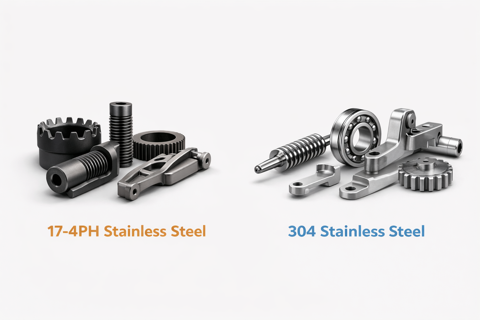
1)Fixture materials are typically stainless steel or high-purity reinforced graphite to prevent volatilization at high temperatures in a vacuum.
2)The fixtures undergo vacuum heat treatment during processing to eliminate residual stresses and ensure dimensional stability and positioning accuracy.
3) The fixtures have adjustable clamping force to effectively reduce the gap between the chip and substrate, minimize solder voids, and ensure sintering quality. Elastic clamping or self-weight clamping with pressure blocks is commonly used.
Vacuum Sintering Equipment
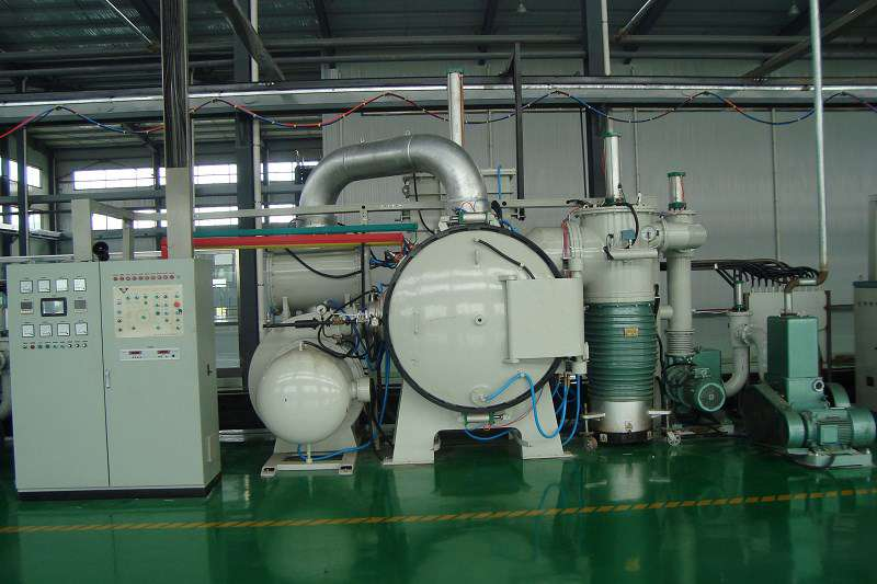
A vacuum sintering furnace is a specialized equipment used for the vacuum sintering and soldering of power hybrid integrated circuits. Taking the RVS-446 vacuum sintering furnace from SIMUWU as an example, it is suitable for batch production in the electronics industry. The main components include the furnace body, heating unit, strong cooling system, vacuum system, and electrical control system.
2.1 Furnace Body
The furnace body is the main part of the vacuum sintering furnace. It consists of a double-layer steel cylinder with a water jacket and an internal heating unit. To meet the cleanliness requirements for component sintering, the inner wall of the cylinder is made of stainless steel, while the outer wall is made of carbon steel. The furnace body is equipped with water-cooled electrodes and introduced thermocouples. The furnace door adopts an elliptical standard head design with an observation window. To ensure vacuum integrity inside the furnace, a dovetail sealing groove and "O"-ring rubber seal are used between the body and the furnace door.
2.2 Strong Cooling System
The strong cooling system is primarily designed to meet the cooling requirements during sintering/soldering. The cooling rate during the solidification of the solder has a significant impact on the quality of the sintered joint surface. Different solders and devices have varying cooling speed requirements. The vacuum sintering furnace is equipped with a dual-function cooling mechanism, utilizing a centrifugal fan and a heat exchanger for rapid cooling. The atmosphere can also be controlled to allow for natural cooling, meeting various process requirements.
Vacuum Sintering Quality
X-ray imaging inspection was performed on Ti-Ni-Ag and Ti-Ni-Au power chips with metallic layers. The X-ray imaging sampling showed minimal voids, and the effective soldering area in batch production exceeded 95%.
Our company is a professional manufacturer of vacuum sintering equipment and related products. With advanced technology and experience, we are able to provide high quality vacuum sintering equipment to meet your needs. Whether it is sintering process or tooling design, we are able to provide you with professional solutions. Our equipment offers reliable performance and excellent stability to ensure weld quality and productivity. If you need any products or services related to vacuum sintering, we will be happy to support and co-operate with you. Please feel free to contact us : edith@xy-global.com , we look forward to working with you to promote the development of the electronics industry.


Share:
Considerations in Metal Injection Molding Manufacturing
Silicon Carbide Vacuum Pressureless Sintering Furnace